
In modern electronics, semiconductor nm is a key measurement. It stands for one billionth of a metre. This size is what makes up the tiny parts in integrated circuits.
The nanometre technology definition is about making things at an atomic level. Making transistors smaller boosts computing power and saves energy.
Knowing about the chip design scale shows us how tech gets better. Every time we shrink the nanometre size, we get a new tech generation.
This basic knowledge helps us see how today’s electronics work. They’re made possible by tiny engineering wonders.
Defining Nanometre Technology and Its Significance
Nanometre technology is a major leap in modern electronics. It changes how we make semiconductors. It works at scales so small, it challenges our usual ideas of size.
The Basics of Nanometre Measurements
A nanometre is one billionth of a metre. It’s incredibly small. For example, a human hair is about 80,000 to 100,000 nanometres wide. This tiny size lets us design electronics with great precision.
Understanding Scale: From Metres to Nanometres
Going from metres to nanometres shows how much semiconductors have shrunk:
- 1 metre = 1,000 millimetres
- 1 millimetre = 1,000 micrometres
- 1 micrometre = 1,000 nanometres
This shrinking lets engineers fit more into smaller spaces. It affects transistor size and chip performance.
Related Posts:


Historical Context of Semiconductor Scaling
The journey to nanometre technology took decades of innovation. In the 1960s, integrated circuits were just micrometres across.
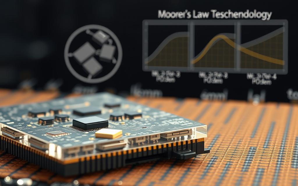
This journey follows Moore’s law. It says transistors on chips double every two years. Gordon Moore made this prediction in 1965, guiding the industry for over 50 years.
Milestones in Technology Shrinkage
The semiconductor history of getting smaller has key moments:
- 1971: Intel 4004 processor with 10μm technology
- 1989: First 1μm process achieved
- 2000s: True nanometre-scale processes start
- 2010s: Commercial production at 14nm and 10nm scales
- 2020s: Development of 3nm and 2nm technologies
Now, we’re aiming for 1nm processes by 2027. This keeps Moore’s law alive, despite big challenges. The shrinking of transistor size has made our powerful computers possible.
What Is NM Technology: Fundamental Concepts
Nanometre technology is a big leap in making semiconductors. It’s a mix of evolution and revolution in design. Working at the atomic level brings new challenges and opportunities.
Transistor Design at the Nanoscale
Today’s transistors are tiny, just a few nanometres wide. They’re the heart of integrated circuits. Their small size means they can pack more computing power into a tiny space.
Size Reduction and Performance Enhancements
Smaller transistors mean faster processing. They switch on and off quicker, making computers faster and using less power. This is key for making devices that are both fast and energy-efficient.
As transistors get smaller, they hit a wall at the atomic level. Here, quantum effects start to play a big role. Engineers face new challenges at this scale.

By controlling electron flow with atomic precision, engineers make these tiny transistors work. The table below shows how size affects transistor performance:
| Transistor Size | Switching Speed | Power Consumption | Components per Chip |
|---|---|---|---|
| 14nm | Moderate | Standard | Billions |
| 7nm | High | Reduced | Tens of billions |
| 5nm | Very High | Significantly reduced | Hundreds of billions |
| 3nm | Extreme | Minimal | Trillions |
Principles Governing Nanometre-Level Engineering
At the atomic level, quantum mechanics takes over from classical physics. This change means new design methods and materials are needed to keep devices reliable.
Quantum Mechanics in Semiconductor Design
Quantum effects become important when transistors are as small as electron wavelengths. These effects bring both challenges and opportunities for engineers.
One key quantum effect is electron tunnelling. It lets electrons pass through barriers that classical physics says they can’t. This can lead to current leaks and lower efficiency.
To deal with these effects, engineers use new materials and designs. They aim to use quantum effects to their advantage. Research in this area is pushing the limits of what’s possible in semiconductors.
The Role of Nanometre Scale in Modern Semiconductors
Nanometre scaling changes how we design semiconductors. It’s not just about making things smaller. It’s about improving how they work and making them cheaper.
Advantages of Smaller Feature Sizes
Getting transistors smaller makes chips better. They work faster and use less power. This helps both the people making chips and those using them.
Improved Speed and Energy Efficiency
Smaller transistors switch on and off quicker and use less energy. This means they can handle more tasks without using too much power. It’s a win-win for everyone.
For example, 5nm chips are 40% better and use the same power as older ones. Or, they can do the same job but use less power. This is great for devices that need to last longer on a charge.
Economic Impacts of NM Technology
Nanometre scaling is a big deal for the economy. It costs a lot to make these chips, but it’s worth it in the long run. Companies that get it right can make a lot of money.
Cost Efficiency and Competitive Edge
Even though making these chips is expensive, they’re cheaper to make in large numbers. More chips can be made from each silicon wafer. This means costs are spread out, making them cheaper overall.
This makes it hard for new companies to get in. But for those who can make these chips, they can charge more and stay ahead.
“The companies that master nanometre scaling first gain approximately two years of market advantage before competitors catch up”
Being an early adopter has big benefits. It shows you’re ahead of the game. This is valuable as the industry keeps getting smaller.
Technological Enablers of NM Scale Design
To reach nanometre scales in semiconductors, we need new ideas. These ideas help us go beyond what was thought possible. We’re seeing big changes in how we make and use materials.
Advanced Lithography Methods
Modern lithography is key for making tiny semiconductors. But, as we get to sizes smaller than atoms, old methods just don’t work.
Extreme Ultraviolet (EUV) Lithography Details
EUV lithography changes how we make tiny circuits. It uses light that’s much shorter than before, at 13.5 nanometres.
Using EUV needs new tools and places. We use mirrors instead of lenses because they don’t absorb the light. And we work in a vacuum to stop the light from scattering.
Big companies are now using EUV in their top lines. This innovation in chip making lets us make things we couldn’t before.
Innovations in Material Science
New ideas in materials are just as important. Old silicon methods hit limits when we get to tiny sizes.
New Materials for Enhanced Performance
Scientists are looking at new semiconductor materials. Things like graphene and transition metal dichalcogenides are very promising. They work well even when they’re just one layer thick.
IBM’s 2-nanometre chip is a big step forward. It uses a new design that improves how well transistors work. This means better performance and less waste.
Looking at new semiconductor materials also helps with heat. As chips get smaller, keeping them cool is more important. This is for their reliability and how well they work.
These advances in making chips and materials are at the forefront of semiconductor technology development. They help us keep up with Moore’s Law and open up new possibilities for computers.
Challenges in Implementing NM Technology
The move to smaller semiconductor nodes faces big hurdles. These challenges test the limits of physics and engineering. NM technology offers great advances but comes with big difficulties in both theory and practice.
Physical and Technical Hurdles
At nanometre scales, old semiconductor physics no longer works. Engineers face new phenomena that were small at larger sizes. These quantum effects make design harder than before.
Quantum Effects and Their Challenges
Quantum tunnelling is a big issue. It lets electrons go through barriers they shouldn’t. This causes current leaks, leading to more power use and heat.
To solve this, makers need to find ways to keep components apart. They also face atomic-scale issues that affect how well things work. As sizes get closer to atoms, these problems get worse.

Manufacturing and Production Difficulties
Switching to nm-scale making brings huge manufacturing challenges. It needs special equipment that costs billions to make.
Precision Requirements and Yield Rates
Nm processes need very precise alignment, in single-digit nanometres. Even tiny changes can mess up production. Keeping everything precise is a huge technical challenge.
This precision affects semiconductor yield rates. Lower yields mean higher costs. Makers must find a balance between new tech and keeping costs down.
| Manufacturing Challenge | Impact on Production | Current Solutions |
|---|---|---|
| Atomic-scale patterning | Requires extreme ultraviolet lithography | Multi-patterning techniques |
| Material purity requirements | Increases material costs significantly | Advanced filtration systems |
| Thermal management | Affects device reliability and longevity | Novel cooling architectures |
| Defect detection | Challenges traditional inspection methods | Machine learning algorithms |
Despite these challenges, the industry keeps finding new ways to solve them. Research and R&D help a lot. Making more chips that work is a big goal for all makers.
Real-World Applications of NM Technology
Nanometre technology is changing our daily lives. It powers devices we use every day. This technology makes devices smaller and more powerful.
Consumer Electronics and Devices
Modern gadgets rely on nm technology. It makes devices smaller and more efficient. This is why our phones and laptops are so powerful today.
Examples in Smartphones and Laptops
Smartphones show nm technology’s impact. They have tiny processors that pack a big punch. This makes them incredibly fast.
Laptops also benefit from nm technology. They are thinner, last longer, and work faster. IBM says its 2 nm tech could make phones and laptops even better.
| Device Type | Performance Improvement | Power Efficiency Gain | Physical Size Reduction |
|---|---|---|---|
| Smartphones | Up to 45% faster processing | 75% less energy consumption | 30% smaller chips |
| Laptops | 60% higher multitasking | 4x battery life extension | 50% thinner designs |
| Tablets | Enhanced graphics rendering | Better thermal management | Lighter construction |
High-Performance Computing
Nm technology also powers the world’s fastest computers. These computers solve problems that normal computers can’t. They are essential for many fields.
Use in Servers and Supercomputers
Data centres use nm technology in their servers. These HPC servers handle huge tasks. They help with AI, weather forecasting, and scientific research.
Supercomputers are the top of this technology. They can do trillions of calculations per second. They help us make new discoveries in medicine and physics.
Nm technology is changing our world. It powers everything from our phones to supercomputers. It drives progress in many areas.
Future Directions for NM Technology
The quest for smaller, faster semiconductors is driving innovation in nanotechnology. As silicon’s limits are reached, researchers are looking at new materials. These could change how we compute and use energy.
Emerging Materials Beyond Silicon
Silicon’s role in semiconductors is facing big challenges at the atomic level. The search for new materials is growing, with several promising options. These could change the future of future nm nodes.
Potential of Graphene and Other Compounds
Graphene is a standout material for beyond silicon uses. It’s a single-layer carbon that’s very conductive and strong. Scientists are working on using graphene in transistors for faster, more efficient computing.
Other materials like molybdenum disulfide and black phosphorus also show great promise. They have properties that silicon can't match at the nanoscale. Questions about nanometer scale semiconductor also connect with affects scientific research accelerating when readers compare closely related topics. By stacking different 2D materials, new electronic properties can be created.

Transition metal dichalcogenides are also getting attention. They have great switching properties and could lead to ultra-thin, flexible electronics. Making these materials work requires new manufacturing methods and designs.
Industry Roadmaps and Future Goals
The semiconductor industry has detailed plans for progress. These roadmaps help align efforts from academia and the private sector. They ensure everyone is working towards the same goals.
Predictions for Next-Generation Nodes
The IEEE’s roadmap says we’ll reach the 1 nm node by 2027. This is a huge step in miniaturisation, needing breakthroughs in many areas.
The semiconductor roadmap sets targets for the future. It includes smaller contact pitches, better interconnects, and new transistor designs. The focus is on making things smaller, faster, and cheaper.
| Projected Node | Expected Timeline | Key Challenges | Potential Solutions |
|---|---|---|---|
| 2 nm | 2024-2025 | Contact resistance | New metallisation schemes |
| 1.5 nm | 2026-2027 | Quantum effects | 2D material integration |
| 1 nm | 2027-2028 | Manufacturing precision | EUV lithography advances |
| Sub-1 nm | 2030+ | Atomic variability | New computational models |
Improving systems is also key, not just making things smaller. Three-dimensional integration, advanced packaging, and co-design are becoming more important. These strategies help improve performance in new ways.
Switching to beyond silicon technologies needs a lot of research and investment. Working together is essential for solving the complex challenges ahead.
Comparative Analysis of NM Technology Generations
To understand nm technology generations, we need to look at technical specs and manufacturer strategies. Moving from larger to smaller nodes is a huge achievement in technology. Anyone researching nanometer scale semiconductor may also want to understand dashboard visualizing data performance before deciding on the best option. This analysis will cover the technical growth and the competitive landscape in semiconductor development.
Progress from 10nm to 3nm Technologies
The move from 10nm to 3nm technology is a big step forward in making semiconductors. Each smaller node size brings better performance and efficiency. The industry keeps pushing limits to achieve these big changes.
Performance Metrics and Comparisons
Key performance indicators show big improvements with each technology generation. Transistor density goes up a lot with each smaller node. At the same time, power use goes down, and processing power goes up a lot.

Looking at performance, smaller nm technologies clearly win. The 7nm vs 5nm vs 3nm comparison shows big improvements in all areas. Each new generation is about 15-20% better than the last at the same power use.
IBM’s research shows even bigger gains at the 2nm level. They say 2nm tech could be 45% faster or use 75% less energy than 7nm tech. These findings show the ongoing promise of shrinking semiconductor sizes.
| Technology Node | Transistor Density (MTr/mm²) | Power Efficiency | Performance Gain |
|---|---|---|---|
| 10nm | 50-100 | 1x Baseline | Reference |
| 7nm | 90-120 | 35% Improvement | 20-25% |
| 5nm | 170-200 | 45% Improvement | 30-35% |
| 3nm | 250-300 | 60% Improvement | 40-45% |
| 2nm (Projected) | 350-400 | 75% Improvement | 45-50% |
Strategies of Key Industry Players
Looking at how leading manufacturers approach nm technology shows different strategies. Intel, TSMC, and Samsung each have their own way of advancing technology. Their competing methods drive innovation across the industry.
Approaches by Intel, TSMC, and Samsung
Intel focuses on designing and making chips together. They aim to improve performance through better design. Recently, they’ve invested in advanced manufacturing to regain their lead.
TSMC focuses on making chips for others. They aim to be the best at manufacturing. Their success comes from focusing on production while others design.
Samsung combines making chips for others with their own production. They use their electronics business to meet their own needs and supply others. This approach gives them both internal and external customers.
Each company’s strategy reflects their unique place in the market. Intel, TSMC, and Samsung show three different ways to compete in advanced manufacturing. Their different methods push technology forward together.
The rivalry among these giants helps everyone. Consumers get better devices, and businesses get more powerful computers. This competition keeps pushing nm technology forward.
Environmental and Societal Aspects
Nanometre technology is advancing fast, but we need to think about its wider effects. We must look at the environmental and ethical sides of making advanced chips, not just their tech achievements.
Sustainability in Semiconductor Production
Making complex chips is tough on the environment. Factories use a lot of water and energy, and the chemicals used can harm the planet. The industry must work on making semiconductor sustainability better.
Energy Use and Environmental Footprint
Creating semiconductors is very energy-intensive. Factories run all day, every day, using lots of power. IBM says data centres use about 1% of the world’s energy.
Switching to smaller chips could save energy. New 2nm processors use less power, which helps the environment. This is a big step towards making tech more sustainable.

Ethical Considerations in Advanced Tech
The rise of powerful tech raises big ethical questions. As chips get smarter and more common, we need to think about their impact on society. This is a job for tech makers, governments, and users.
Privacy, Security, and Societal Impact
Advanced chips can process data like never before, but this brings risks. They power important medical devices but also help with surveillance. We need to think carefully about how to use this tech.
New privacy security chips help protect our data, but they also create new risks. The fact that most chips are made in a few places can cause problems. It leads to global tensions and risks in getting tech.
We must be careful as we make tech more powerful. We need clear policies and work together globally. This way, we can enjoy the benefits of tech without harming society or individuals.
Influence of NM Technology on Other Sectors
Nanometre-scale technology has changed many fields, not just computers. It’s making big changes in healthcare, transport, and space. These changes come from better semiconductor solutions.
Advances in Healthcare Technology
Nanometre technology has led to big steps forward in medicine. It makes devices smaller and more precise. This means we can have advanced healthcare in more places.
Applications in Medical Imaging and Devices
Modern medical imaging uses nanometre technology for better pictures. MRI and CT scanners now have medical technology chips for fast, clear images. This helps doctors make accurate diagnoses.
There’s also a big leap in portable diagnostic devices. These small tools use nanometre tech for lab-quality tests outside hospitals.
“The use of nanometre-scale semiconductors in medical devices has cut down diagnostic time. It’s now minutes instead of hours, and it’s much more accurate.”
Here’s a table showing how nanometre technology is changing healthcare:
| Application Area | NM Technology Contribution | Impact Level |
|---|---|---|
| Medical Imaging Systems | Higher resolution sensors | Revolutionary |
| Portable Diagnostics | Miniaturised processing units | Transformative |
| Implantable Devices | Reduced power consumption | Significant |
| Telemedicine Equipment | Enhanced data transmission | Substantial |
Impact on Automotive and Aerospace Industries
The car and space industries are using nanometre technology for better cars and planes. They get chips that work well but are small and use little power.
Enhancements in Vehicle and Aircraft Systems
Today’s cars have automotive semiconductors for smart features. These chips handle lots of data fast. This means cars can:
- avoid crashes
- keep a safe distance
- stay in their lane
- park by themselves
In self-driving cars, these chips make quick decisions. They need to process lots of data at once. This is only possible with nanometre tech.
Space tech also gets better with aerospace avionics. Modern planes use nanometre parts in:
- controlling the plane
- finding their way
- managing the engines
- keeping passengers entertained
This leads to safer, more fuel-efficient, and better travel experiences in cars and planes.
Conclusion
Nanometre technology is key to today’s semiconductor design. It boosts performance, efficiency, and innovation in many devices. This is true for everything from smartphones to supercomputers.
The future of semiconductors will keep improving thanks to nanoscale advancements. New materials and processes will lead to more breakthroughs. These will help in healthcare, cars, and more.
Nm technology is vital for our tech’s growth. It shapes industry plans and sparks new ideas. Its impact shows how important it is in our fast-changing world.
FAQ
What is a nanometre and why is it important in semiconductor design?
A nanometre (nm) is one billionth of a metre. In chip design, it shows the size of transistors. This size affects how fast and efficient devices are.
Smaller nm sizes mean more transistors in a smaller space. This boosts speed and cuts down energy use.
How has semiconductor scaling evolved over time?
Scaling has moved from micrometres to nanometres. This change follows Moore’s Law, which says transistors double every two years.
Big steps include going below 100nm and aiming for 7nm, 5nm, and 3nm.
What are the main benefits of smaller nm technology in chips?
Smaller nm tech brings many benefits. It means more transistors, faster processing, and less power use.
This leads to more powerful and energy-saving devices. It also makes devices cheaper over time.
What challenges arise when working at the nanometre scale?
At nanometre scales, quantum effects like electron tunnelling cause problems. These include current leaks and less reliability.
Also, making chips at this scale is very hard. It needs super-accurate processes and a lot of money for research and making chips.
How does Extreme Ultraviolet (EUV) lithography support nm technology?
EUV lithography is key for making tiny features. It uses short-wavelength light for finer patterns than old methods.
This lets us make transistors for advanced nodes like 7nm and below.
Which companies are leading in nm technology development?
Intel, TSMC, and Samsung are leading in making chips. They use different ways like EUV and new materials to stay ahead.
This drives innovation and sets new standards in the industry.
In which industries is nm technology having the biggest impact?
Nm tech is changing many fields. It’s making devices like smartphones more powerful. It’s also key for AI, cloud computing, healthcare, cars, and planes.
It helps in medical imaging, driver-assistance systems, and more.
What role does material science play in advancing nm technology?
Material science is vital for pushing past silicon limits. New materials like graphene and transition metal dichalcogenides improve performance.
They help in making chips smaller and better for the future.
How does nm technology affect sustainability and the environment?
Nm tech makes devices more energy-efficient. But making chips is very energy-hungry and pollutes.
The industry is working on being greener. It wants to use less water, manage waste better, and make plants more energy-efficient.
What ethical considerations are associated with advanced nm technology?
Nm tech raises big ethical questions. It makes devices more powerful, which can be a problem for privacy and security.
It can also lead to more surveillance and make it harder to protect data. We need to innovate responsibly and have strong rules.